
Copper-Indium-Gallium-Selenide technology was expected to revolutionize the industry. What happened — and how it can make a comeback.
By Brad Mattson, Special To Solar Power World
One of the most interesting and controversial materials in solar is Copper-Indium-Gallium-Selenide, or CIGS for short. It was part of a solar thin-film-hype cycle where some CIGS companies such as Solyndra, NanoSolar and MiaSolé almost became household names. These combined companies alone accounted for over $1 billion in venture capital investment. With all that money and all that excitement, what happened? Two of those companies no longer exist, and the third was sold for less than 10 cents on the invested dollar. Yet despite a dark cloud over the technology, there is still a silver lining.
CIGS’ Silver Lining
The good news? CIGS is a demonstrably capable and versatile material. The world records for thin-film efficiency are all held by CIGS. Even though a-Si and CdTe (the other thin-film technologies) have continually improved their efficiency, CIGS has improved as well and maintained distinct advantage. Just recently, polycrystalline CIGS achieved higher efficiencies than polycrystalline silicon with a world record of 20.8% compared to 20.4% for silicon. This is significant. It opens up the possibility of the holy grail in solar: Silicon-like efficiencies at low thin-film costs.
CIGS is the only technology that offers this promise.
CIGS is also versatile. There are many forms of the material that work well and many ways to make it. CIGS can be made by the following processing techniques: sputtering, evaporation, electrochemical deposition, nanoparticle printing and ion-beam deposition. In addition, sputtering can be a two-step process (sputter first, react with selenium later), or a single-step reactive sputtering process. Evaporation is similar in that one can use a single stage, two-stage or three-stage evaporation process. The variations don’t stop there. CIGS material can be deposited on many substrates: glass, plastic, stainless steel and aluminum. This versatility provides many pathways to an optimal solution.
Here’s The Problem
This versatility provides many pathways to an optimal solution. Unfortunately, versatility led to almost every pathway being explored, and, as you might expect, many pathways had dead ends. In striving for differentiation, technologies were developed that sounded promising but delivered no real value. In the end, physics rules — and there is really one optimal process based on achieving the highest performance at the lowest costs. Let’s look at these choices and what happened.
With CIGS there are three distinct technology choices that lead to success or failure: simultaneous vs. two-step process, single-stage or multi-stage deposition and device architecture. The industry tends to focus only on material technology (c-Si vs. CdTe vs. CIGS), but it may be the process and architectural decisions, independent of material, that make the biggest difference.
Looking first at one-step vs. two-step processing provides the first filter in our process selection. In the single-step process, CIGS is deposited all four materials (Cu-In-Ga-Se) at once. In the two-step process the Copper, Indium and Gallium are first deposited in a “rough” form, not the final desirable crystal structure. Then, in a second step, the 4th and often a 5th material, Se and S are added in a “selenization/(sulfurization)” step where the deposited layer is recrystallized to the final desirable form.
Basically, the two-step process is flawed from both a performance and cost perspective. The original idea was that the first step of the two could be done cheaply, avoiding the more costly single-step process. Unfortunately, even if the first step was really cheap, like nanoparticle printing, the second step was much more expensive. Any savings in the first step was lost in the second step. Worse than that, the efficiency has always been lower than gold standard — co-evaporation, which is a single-step process. So lower efficiency and higher cost means the two-step process is not a formula for success.
One-Step Process
The single-step processes are reactive sputtering (sputter Cu-In-Ga in a Selenium ambient), and the various co-evaporation processes: single-stage, two-stage, and three-stage co-evaporation. This is the second filter in the process selection. Explaining this selection requires a little diversion into solar-cell device physics.
The absorber (the CIGS layer) in a solar cell is where the action is. Here, the light is absorbed and, through the photovoltaic effect, an electron-hole pair is created. The objective is to collect that electron before it runs into something and is re-absorbed (called recombination). This collection of electrons becomes the electricity we use to light a light bulb. It turns out electrons want to recombine in the bulk CIGS material itself as well as at interfaces with other materials.
The perfect solar material would be optimized to maximize generation of electrons in the bulk material, but minimize recombination in the bulk as well as at each of the interfaces. If one were lucky, a single material would be perfect for all of these jobs. So far though, no one has encountered this perfect material. With silicon, the mainstay of solar technology, the bulk properties are altered at both the top and bottom contact to maximize efficiency. It turns out CIGS can do that too, but only in the three-stage co-evaporation process.
The stages in the co-evaporation process can be thought of as zones of deposition. If multiple stages are employed, the materials properties can be adjusted throughout its thickness; the more zones, the more process control. Therefore, a three-stage co-evaporation can be optimized for good absorption with minimal recombination in the bulk, but with different material properties at the top and bottom contact to minimize recombination at these interfaces. It is no surprise that the world records for efficiency over the last 10 or more years are all accomplished with three-stage co-evaporation.
It is clear that three-stage co-evaporation is preferred, but it is also true that this process takes the most skill to implement. The processing tool is more complicated than a simple sputtering or nanoparticle printing system, but avoiding this process leads to sub-optimal results. There is just no better way to do it.
It’s All In The Architecture
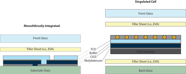
The last decision when implementing a CIGS process is the architecture of the device and the manufacturing process flow. Choices are:
- cells vs. monolithically interconnected (MLI) panels,
- substrate material-size/shape
- rigid vs. flexible and
- manufacturing process flow.
This decision may have had more to do with the success and failure of CIGS companies than anything to do with CIGS as a material. For example, the cylindrical substrate used at Solyndra doomed the technology from the beginning. Solyndra was not a CIGS failure, but an architecture failure.
The first major decision is whether or not to make individual solar cells — the choice between singulated cells vs. MLI. With singulated cells, the manufacturing process is similar to that of silicon solar panels, where small solar cells are fabricated and then large numbers of them are strung together and laminated between glass and a backsheet to form a module. In MLI, cells are not fabricated individually. Rather, they are formed all at the same time, typically on a glass substrate. This is the simplest process flow with both the fewest steps and the fewest materials needed — and therefore the lowest cost.
Selecting MLI usually leads to a rigid glass substrate, but with singulated cells one can employ a flexible substrate with a roll-to-roll (R2R) manufacturing process. This was the choice in many high profile companies: NanoSolar, Miasole, SoloPower, Global Solar, Solarion and NuvoSun. At first, R2R looks attractive. Imagine the high-speed processes of a paper mill, steel mill or textile factory.
Unfortunately, the throughput never matched the expectation, and current R2R production lines have roughly the same throughput as rigid-glass lines. In fact, because the industry standard (c-Si) is a laminated glass product, the R2R process just adds more process steps and requires more materials than the simple MLI process. And that’s not all. If the substrate is metal (almost all the above are), thanks to electrical flaws (called shunts) the R2R process requires the addition of diodes in the panel to avoid failures, adding further cost and complexity.
To add insult to injury, depositing on metal substrates generally results in lower efficiency than depositing on glass substrates. So R2R was a great idea except:
- It adds complexity and process steps
- It adds more materials
- It requires diodes
- It results in lower efficiency
It is no surprise that of all the R2R companies formed, almost none have survived as independent entities. They have either died, been purchased or are being sold right now.
The earlier process selection was pretty clear, and it turns out the architectural selection is also clear: MLI on glass is the best choice. All other choices tried have not succeeded. In fact, the only thin-film companies in the world that have scaled beyond 150 MW, First Solar and Solar Frontier, are both MLI on glass. That data speaks for itself.
In summation, there are so many options to produce CIGS that a roadmap is needed. But careful analysis of the basic physics and what has worked in the past narrows down the choices. It turns out that the optimal choice is now clear; three-stage co-evaporation with monolithic integration on glass not only results in the best process at the lowest cost, it has the promise of reaching silicon efficiencies at thin film costs. In fact, it might be the only technology that can get us to the fabled land of a sustainable $0.40/watt.
Brad Mattson, CEO of Siva Power (formerly Solexant), is a thin-film module company that is implementing CIGS technology on the largest scale process line in the world. To hear him talk about CIGS and the manufacturing process Siva Power is putting together, listen to his Solar Speaks podcast with Editorial Director Frank Andorka.


Tell Us What You Think!